Wafer Bumping Machines for Assembly Process Interconnections
Wafer bumping is often separated into two different categories: Flip chip bumping (FC) and wafer level chip scale packaging (WLCSP). This categorization and affiliated nomenclature is partially based on the solder bump size and the type of equipment used to create the bump.
The basic flow for each of these technologies is to first deposit a barrier metal on top of the bond pad of the wafer (Under-Bump Metallization or UBM) followed by deposition of the solder. Possible Solder Alloys:

Wafer Bumping Equipment
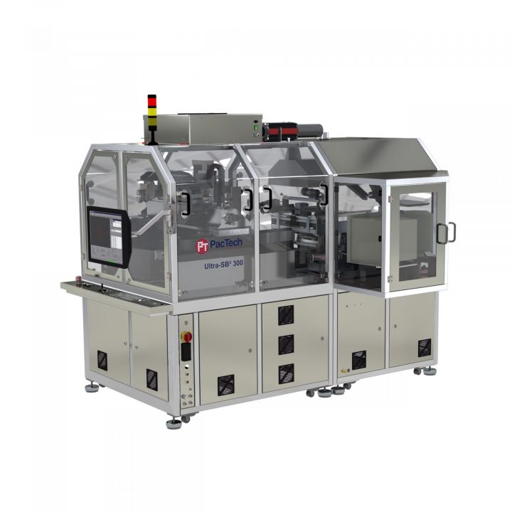
Ultra-SB² ®
Ultra-SB² ® is a fully automated solder bumping equipment integrating flux printing, ball placement, 2D inspection and wafer level rework.
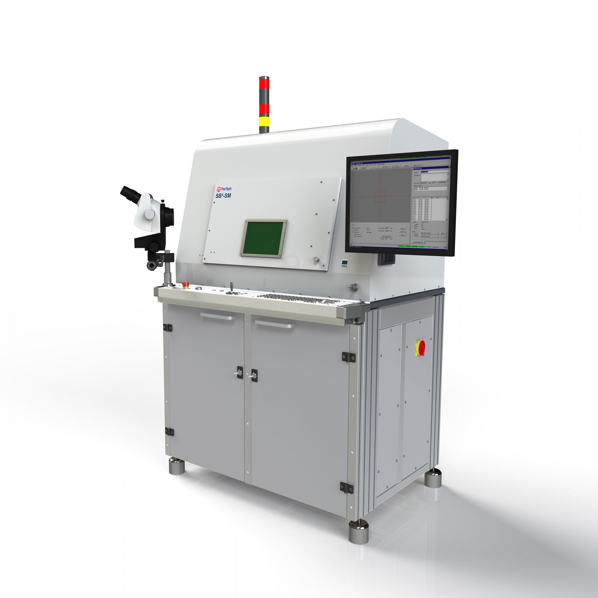
SB² ® – SM
The SB² ® - SM is a machine for prototyping and small volume production that has wider working area than the SB² ® - M and more optional features.
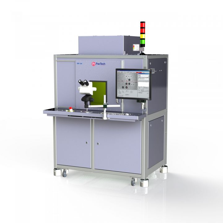
SB² ® – Jet
SB² ® - Jet offers the highest placement precision of all PacTech machines and is capable of processing the smallest solder balls in the portfolio.
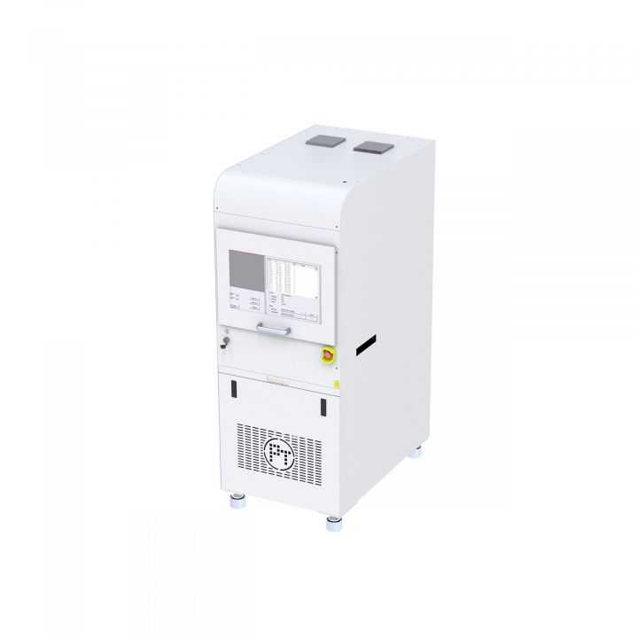
SB² ® – Compact
SB² ® – Compact machine is the SB² ® entry point for high volume production with highly flexible and ultra-compact workstation.