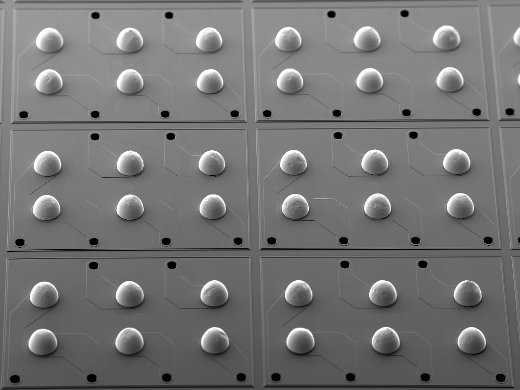
SOLDER BALLING SERVICE
PacTech uses an electroless nickel plating process to deposit the Under-Bump-Metallurgy (UBM) and three different technologies to deposit / rework the solder spheres:
The choice between these solder deposition technologies is based on product type, bump height requirements, pad pitch, and volumes to be bumped.
Flip Chip Bumping and WLCSP Bumping Overview:
Wafer bumping is often separated into two different categories: flip chip bumping (FC) and wafer level chip scale packaging (WLCSP). This categorization and affiliated nomenclature is partially based on the solder bump size and the type of equipment used to create the bump.
“Flip Chip” refers to bumps on semiconductor wafers which are in the range of 50 to 200 µm in height and are usually assembled using and underfill material between the die and the substrate.
“WLCSP” refers to bumps that are in the range of 200 to 500 µm in height and are usually assembled without an underfill material.

