LASER ASSISTED BONDING SERVICE

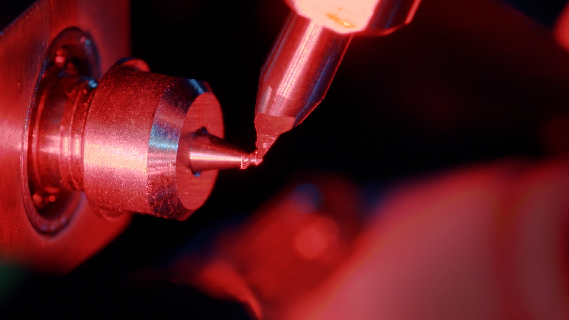
The majority of today’s Flip chip bonders are derived from modified surface mount equipment. This method of flip chip attach uses thermal energy to reflow the bumped chip to the substrate.  The advantage of laser heating instead of direct thermal heating is given by high selectivity with an extremely good time control in the millisecond time range. This is in contrast to infrared and convection ovens where the assembly process takes minutes. By using the laser to reflow the solder bumps, the thermal stress induced in the package and on the substrate is minimized allowing implementation of new substrates and new IC’s which are thermally more sensitive.

Process cycle times are improved by the equipment concept of performing chip placement and assembly reflow simultaneously and the absence of long heating and cooling cycles of standard TCB bonder systems. Beside of this the process capability for ACF, NCP and solder interconnection techniques illustrates the high flexibility of the laser heating process.
Download WLP Brochure
Get in Contact with Sales
Laser Assisted Bonding Service

WAFER LEVEL PACKAGING SERVICES

Electroplating

Electroplating, or electrochemical deposition, is the process of using electrodeposition to coat an object in a layer of metal(s) on any substrate. RDL and Copper for example, are part of this process.

Go to Electroplating Service

Electroless-Plating

Low-cost mask-less chemical deposition of various metal stacks on wafer surface to serve as intermetallic connection or to enhance product reliability and performance.

Go to Electroless-Plating Service

Laser Assisted Bonding

Laser assisted bonding is an interconnection method performed through the laser energy to bond two surfaces of materials together.

Go to Laser Assisted Bonding Service

Solder Balling

Various solder deposition technologies to form solder bump for WLCSP and flip chip interconnects.

Go to Solder Balling Service

Wafer Level Component Assembly

Wafer level assembly by attaching of dies or various passive components on wafer surface.

Go to WL Component Assembly Service

Wafer Thinning

Thinning of wafer backside for dies in final packaging.

Go to Wafer Thinning Service

Wafer Metal Coating

Application of various metal stacks via evaporation or sputtering technologies on wafer backside for better die performance.

Go to Wafer Metal Coating Service

Wafer Dicing

High precision and accurate singulation of dies on a wafer.

Go to Wafer Dicing Service