WAFER METAL COATING SERVICE

For better chip performance in terms of contact resistance and heat dissipation, metallizing the backside of the wafer has proven to be very effective. PacTech Asia uses an e-beam evaporation technology for its wafer backside metallization. The benefits of this technology are speed and low contamination as only the electron beam touches the source material.

We have the capability of coating metals on wafers using the evaporation process with less than 20% variation on the metal thickness (wafer-to-wafer as well as within the overall wafer). This process deposits single or multi-layer of thin metal films on controlled thickness using an electron beam gun (e-gun) evaporation source. We also provide options of mirror and matte finish depending on customer’s requirement.
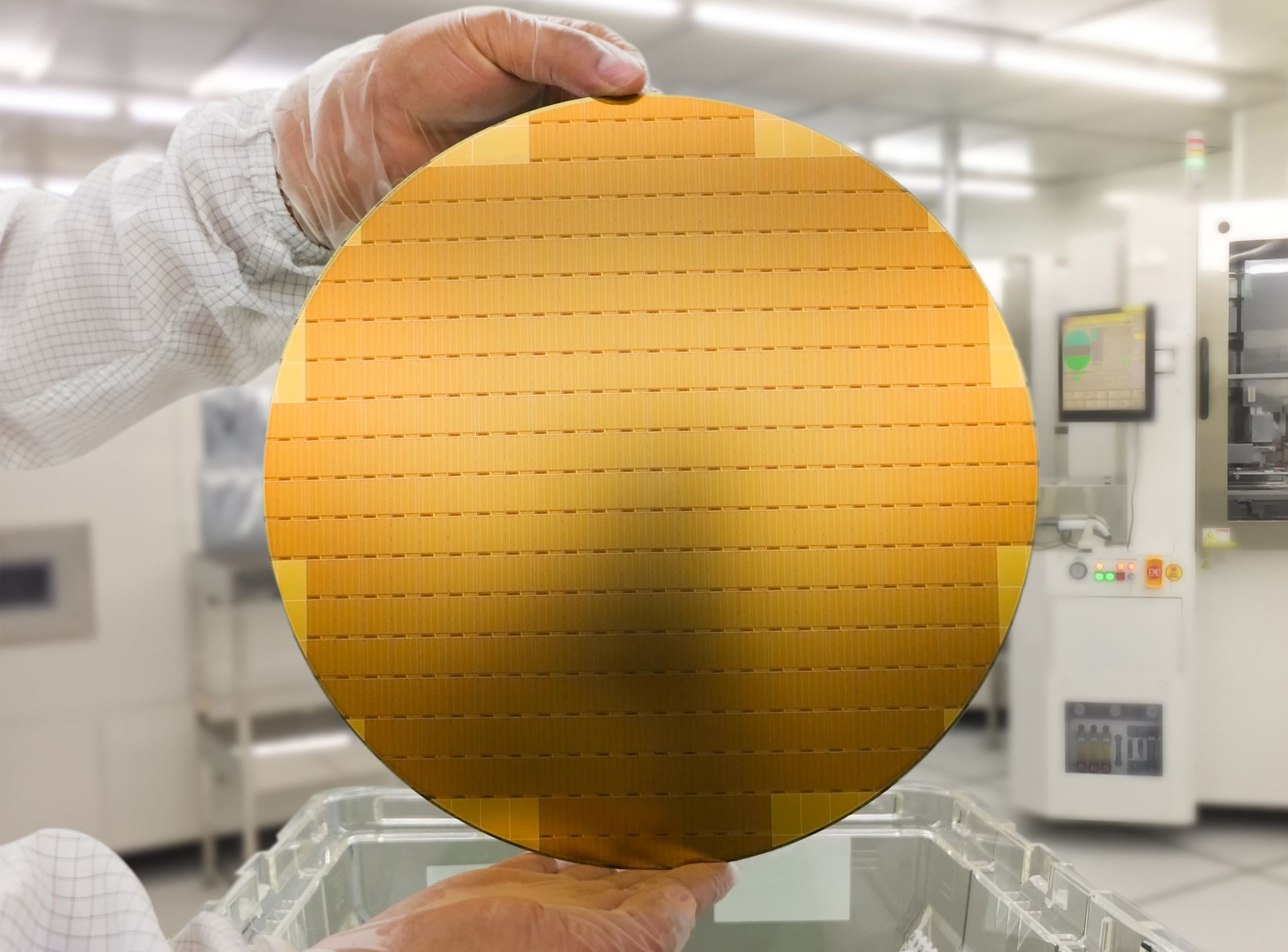
Wafer Metal Coating

WAFER LEVEL PACKAGING SERVICES

Electroplating

Electroplating, or electrochemical deposition, is the process of using electrodeposition to coat an object in a layer of metal(s) on any substrate. RDL and Copper for example, are part of this process.

Electroless-Plating

Low-cost mask-less chemical deposition of various metal stacks on wafer surface to serve as intermetallic connection or to enhance product reliability and performance.

Laser Assisted Bonding

Laser assisted bonding is an interconnection method performed through the laser energy to bond two surfaces of materials together.

Solder Balling

Various solder deposition technologies to form solder bump for WLCSP and flip chip interconnects.

Wafer Level Component Assembly

Wafer level assembly by attaching of dies or various passive components on wafer surface.

Wafer Thinning

Thinning of wafer backside for dies in final packaging.

Wafer Metal Coating

Application of various metal stacks via evaporation or sputtering technologies on wafer backside for better die performance.

Wafer Dicing

High precision and accurate singulation of dies on a wafer.