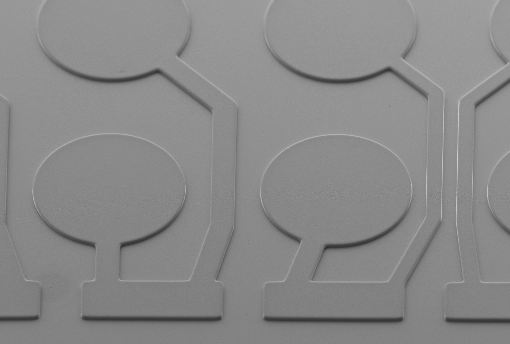
REDISTRIBUTION LAYER (RDL) SERVICE
Many dies are not designed for flip chip or wafer level chip scale packaging. The bond pads of many dies are designed as a peripheral row near the edge of the die. These bond pads are typically designed for wirebonding applications and are therefore often too small for solder bumping. Reconfiguring or redistributing these pads from the perimeter footprint to alternative locations on the chip enables wafer bumping (flip chip or WLCSP).
The use of redistribution layer allows utilization of greater area of the chip resulting in significant area savings, common I/O footprints, and enables the use of simpler, less expensive substrates. The first process step for redistribution is the deposition of a dielectric layer on the wafer to enhance the die passivation followed by metals trace to reroute the pads to new locations.

