ELECTROLESS PLATING SERVICE

PacTech offers subcontractor electroless nickel plating services for wafer bumping, pad redistribution and ACF/ACA applications. PacTech has three manufacturing sites around the world which offer these services. Our goal is to be customer oriented and flexible to meet all the customer’s needs. We offer support for prototyping, engineering, and R&D projects as well as high volume production. Each PacTech facility has a throughput of 600,000 wafers per year.

PacTech offers several different pad finshes and layer thicknesses using electroless nickel plating in combination with electroless palladium and immersion gold process:

  • e-Ni/Au
  • e-Ni/Pd
  • e-Ni/Pd/Au
  • e-Ni/Ag

Our flexible process is able to deposit nickel thicknesses between 2µm and 25µm, depending on the requirements and application. Palladium can be deposited in the range of 100nm and 300nm, gold is typically deposited between 30nm and 100nm. Running this process for more than 25 years we are very happy to help finding the right specifications for your application.
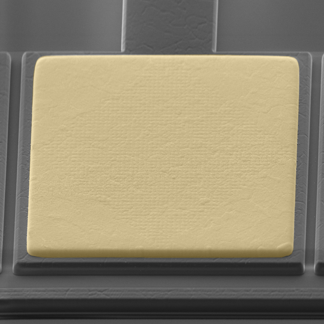
UBM Electroless Plating

WAFER LEVEL PACKAGING SERVICES

Electroplating

Electroplating, or electrochemical deposition, is the process of using electrodeposition to coat an object in a layer of metal(s) on any substrate. RDL and Copper for example, are part of this process.

Electroless-Plating

Low-cost mask-less chemical deposition of various metal stacks on wafer surface to serve as intermetallic connection or to enhance product reliability and performance.

Laser Assisted Bonding

Laser assisted bonding is an interconnection method performed through the laser energy to bond two surfaces of materials together.

Solder Balling

Various solder deposition technologies to form solder bump for WLCSP and flip chip interconnects.

Wafer Level Component Assembly

Wafer level assembly by attaching of dies or various passive components on wafer surface.

Wafer Thinning

Thinning of wafer backside for dies in final packaging.

Wafer Metal Coating

Application of various metal stacks via evaporation or sputtering technologies on wafer backside for better die performance.

Wafer Dicing

High precision and accurate singulation of dies on a wafer.