WAFER LEVEL COMPONENT ASSEMBLY SERVICE

Wafer-level component assembly can result in significant cost savings and shorten cycle time while reducing package size. Our wafer-level component assembly includes solder application, component placement and reflow process, and optional optical inspection. The types of components that can be placed on the wafer include single chips, diodes, capacitors, transistors and other IPD that can directly form a package through wafer-level assembly. The wafer can then be cut into multiple dies and shipped either on a saw ring or taped onto reels for the rest of the assembly process.

Our wafer level component assembly services include:
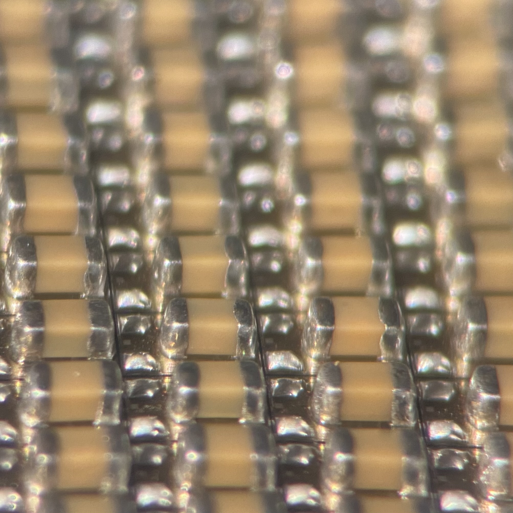
  • High throughput low-cost wafer level component assembly
  • High accuracy low stress LAPLACE laser assisted bonding component attach
Wafer Component Assembly

WAFER LEVEL PACKAGING SERVICES

Electroplating

Electroplating, or electrochemical deposition, is the process of using electrodeposition to coat an object in a layer of metal(s) on any substrate. RDL and Copper for example, are part of this process.

Electroless-Plating

Low-cost mask-less chemical deposition of various metal stacks on wafer surface to serve as intermetallic connection or to enhance product reliability and performance.

Laser Assisted Bonding

Laser assisted bonding is an interconnection method performed through the laser energy to bond two surfaces of materials together.

Solder Balling

Various solder deposition technologies to form solder bump for WLCSP and flip chip interconnects.

Wafer Level Component Assembly

Wafer level assembly by attaching of dies or various passive components on wafer surface.

Wafer Thinning

Thinning of wafer backside for dies in final packaging.

Wafer Metal Coating

Application of various metal stacks via evaporation or sputtering technologies on wafer backside for better die performance.

Wafer Dicing

High precision and accurate singulation of dies on a wafer.