Skip to content
PacTech – Packaging Technology Equipment & Services Logo
  • HOME
  • ABOUT
    • ABOUT PACTECH
    • NEWS
    • EVENTS & EXHIBITIONS
    • CAREER / JOBS
    • PUBLICATIONS
    • LOCATIONS & CERTIFICATES
    • MEDIA LIBRARY
  • EQUIPMENT

    • BY PROCESS
      • Laser Soldering
      • Laser Assisted Bonding
      • Electroless Plating
      • Solder Ball Mounting
      • Wire Soldering

    • BY APPLICATION
      • 3D Packaging
      • Flip Chip
      • Probe Card
      • Reballing
      • SMT

    • BY SECTOR
      • Aerospace
      • Automotive
      • Consumer Electronics
      • Energy and Solar
      • Medical
      • Production and Assembly
    • SB2 RSP Machine

    • PRODUCT FAMILY
      • SB²
      • LaPlace
      • Ultra SB²
      • PacLine
  • WLP SERVICE
    • Electroless Plating

      Electroless Plating

      Electroless Plating – Maskless chemical deposition of metal stacks on wafers as intermetallic connection or to enhance product reliability.

    • Electroplating

      Electroplating

      Electroplating is the process of using electrodeposition to coat an object in a layer of metal(s) on any substrate.

    • Copper Pillar

      Copper Pillar

      Electroplated Cu pillar with optional Ni diffusion barrier and SnAg cap for low cost and fine-pitch flip chip interconnects.

    • Redistribution Layer (RDL)

      Redistribution Layer (RDL)

      Rerouting of pads on a die with metal and dielectric layers to the other locations to fulfil the subsequent packaging rules.

    • Solder Balling

      Solder Balling

      Various solder deposition technologies to form solder bump for wafer level chip scale packaging and flip chip interconnects.

    • Laser Assisted Bonding

      Laser Asssisted Bonding

      Laser assisted bonding is an interconnection method performed through the laser energy to bond two surfaces of materials together.

    • Wafer Level Component Assembly

      Wafer Level Component Assembly

      We offer wafer level component assembly by attaching dies, chips or various passive components like capacitors on a wafer surface.

    • Wafer Thinning

      Wafer Thinning

      Removal of wafer backside materials for thinner die in final packaging via high quality mechanical polishing and chemical stress relief.

    • Wafer Metal Coating

      Wafer Metal Coating

      Application of various metal stacks via evaporation or sputtering technologies on wafer backside for better die performance.

    • Wafer Dicing

      Wafer Dicing

      Wafer dicing is the process where silicon chips (die) are separated from each other on the wafer, accomplished by mechanically sawing.

  • CHEMICALS
  • CONTACT
    • Contact
    • Field Service for Equipment
    • Global Sales Team
  • CUSTOMER CENTER
  • English
    • Deutsch
    • 日本語
  • English
    • Deutsch (German)
    • 日本語 (Japanese)
  • HOME
  • ABOUT
    • ABOUT PACTECH
    • NEWS
    • EVENTS & EXHIBITIONS
    • CAREER / JOBS
    • PUBLICATIONS
    • LOCATIONS & CERTIFICATES
    • MEDIA LIBRARY
  • EQUIPMENT
    • BY PROCESS
      • Laser Soldering
      • Laser Assisted Bonding
      • Electroless Plating
      • Solder Ball Mounting
      • Wire Soldering
    • BY APPLICATION
      • 3D Packaging
      • Flip Chip
      • Probe Card
      • Reballing
      • SMT
    • BY SECTOR
      • Aerospace
      • Automotive
      • Consumer Electronics
      • Energy and Solar
      • Medical
      • Production and Assembly
    • PRODUCT FAMILY
      • SB²
      • LaPlace
      • Ultra SB²
      • PacLine
  • WLP SERVICE
    • Electroless Plating
    • Electroplating
    • Copper Pillar
    • Redistribution Layer (RDL)
    • Solder Balling
    • Laser Asssisted Bonding
    • Wafer Level Component Assembly
    • Wafer Thinning
    • Wafer Metal Coating
    • Wafer Dicing
  • CHEMICALS
  • CONTACT
    • Contact
    • Field Service for Equipment
    • Global Sales Team
  • CUSTOMER CENTER
About Us – PacTechP0-kito_472023-02-06T11:47:53+01:00
PT Logo_PT Weiß

PACKAGING TECHNOLOGIES

Who are we?

PacTech is a technology-focused company specialized in advanced packaging equipment manufacturing and wafer level packaging services. Since our establishment, our team has been working relentlessly on developing new leading-edge technologies for the next generation applications. We are known to be highly adaptive to customization and unique applications. Our team of technical experts is striving to resolve various packaging challenges faced by the industry to provide our customers and partners more competitive solutions in terms of cost, time-to-market, and technology advancement. Our headquarter is located in Nauen, Germany with two operation and manufacturing sites in Santa Clara, CA, USA and Penang, Malaysia. Together with our sales and field service teams across the globe, we can cater to the demand within your region.
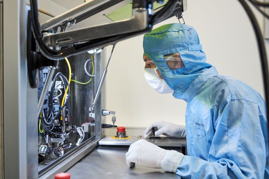
Advanced Packaging Machine Inspection
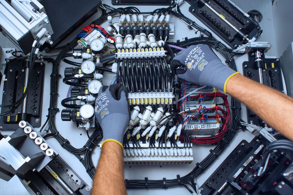
Advanced Packaging Machine from the inside

ADVANCED PACKAGING EQUIPMENT

Our advanced packaging equipment portfolio incorporates several core technologies including laser soldering and wire soldering, laser assisted bonding and innovative wafer level bumping solutions such as electroless plating and wafer level ball placement. We offer equipment solutions for high throughput and fully automated manufacturing as well as advanced research and development field work.

WAFER LEVEL PACKAGING SERVICES

With our state-of-the-art wafer level bumping, metallization, and advanced packaging processes PacTech supports the heterogeneous integration technology roadmap. In combination with our unique laser soldering and laser bonding equipment, PacTech is able to offer a variety of manufacturing and engineering solutions for the technical and economic challenges in today’s industry.  Our manufacturing sites are ISO 9001 and IATF 16949 certified for highest level of quality and process control. Being a socially responsible company, we are also ISO 14001 and ISO 50001 certified for our operations.
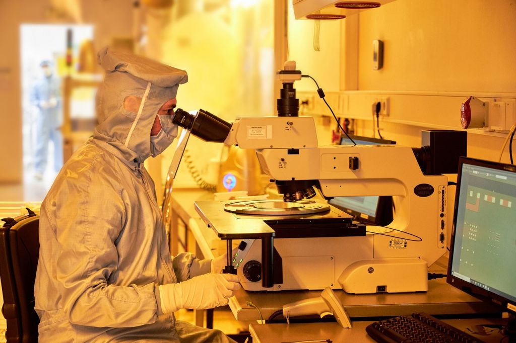
Clean Room Wafer Inspection
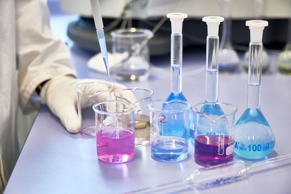
Mixing Plating Chemicals

Chemicals

As a turnkey solution provider for electroless plating, we are supplying complete process solutions to our customers by combining our plating know-how, equipment and process chemicals to guarantee a successful process transfer. Our plating chemicals are controlled by highest quality standards and are available throughout a worldwide distribution network to handle import and warehousing task, but also to provide technical onsite support to our customers.

0
Employees
0+
Machines Produced
0+
Patents

PacTech History

1995 - Foundation

Berlin, Germany, as spin-off from Fraunhofer-IZM

1997 - 1st Manufacturing Facility

PacTech GmbH, Nauen, Germany

2001 - 2nd Manufacturing Facility

PacTech USA Inc., CA, USA

2003 - Key Supplier

for Hard Drive Soldering (HGA, HSA)

2008 - 3rd Manufacturing Facility

PacTech Asia Sdn. Bhd., Malaysia

2012 - Key Supplier

for Camera Module Soldering

2015 - Demo Center

Opening in Shanghai, China

2015 - 100% Owned

by Nagase & Co. Ltd.

2017 - Key Supplier

for Solar Cell Production in China

2022 - Achievements to Date

> 2.000 Production Machines shipped
> 165 patents granted
~ 420 employees

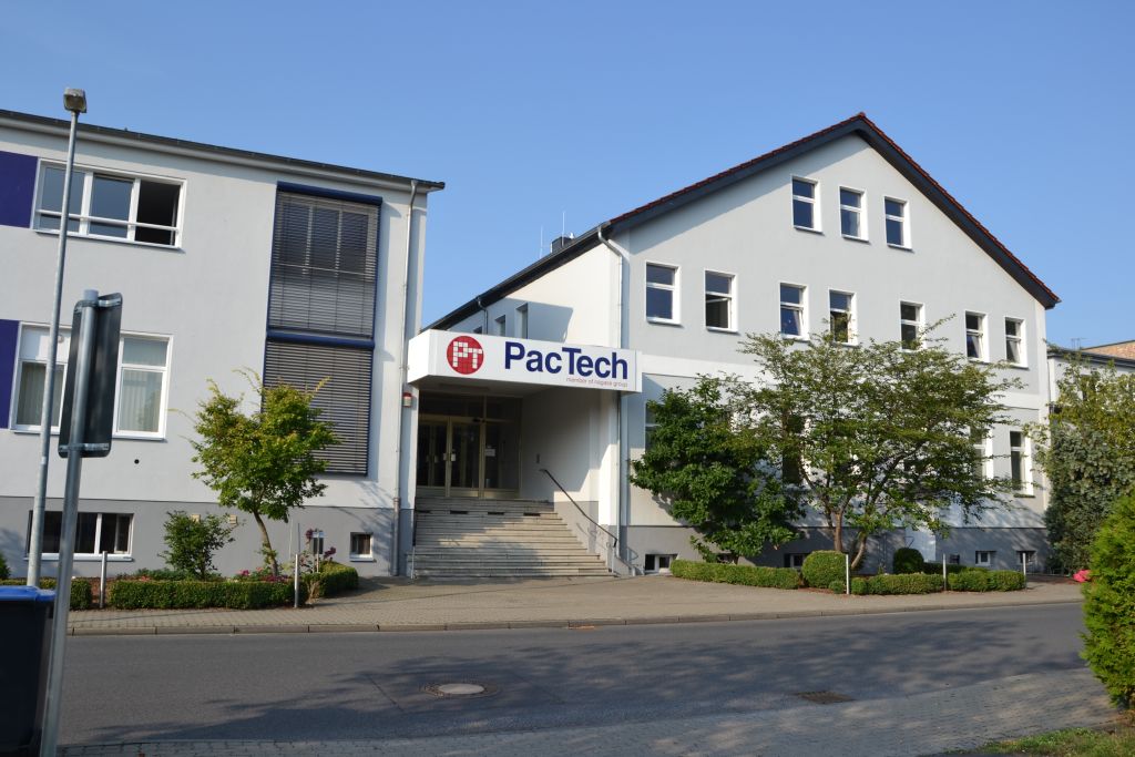
PacTech Building Nauen

PacTech Management

Dr. Thorsten Teutsch
Managing Director | CEO

Annette Burczyk
Annette Burczyk
Managing Director | CFO
Dipl.-Ing. Thomas Oppert
Vice President | Global Sales & Marketing
Thorsten Krause
Thorsten Krause
Business Unit Manager Equipment
Matthias Fettke
Matthias Fettke
Business Unit Manager Service & Application
Ricardo Geelhaar
Ricardo Geelhaar
Business Unit Manager Wafer Level Packaging

NEWSLETTER

NAVIGATION

Jobs

Contact

Locations

Imprint

Terms & Conditions

Privacy Policy

Cookie Policy

© PacTech - Packaging Technologies GmbH 2012 - 2022 | All Rights Reserved |
  Member Of NAGASE Group
Page load link
PacTech - Packaging Technology Equipment & Services
Manage Cookie Consent
To provide the best experiences, we use technologies like cookies to store and/or access device information. Consenting to these technologies will allow us to process data such as browsing behavior or unique IDs on this site. Not consenting or withdrawing consent, may adversely affect certain features and functions.
Functional Always active
The technical storage or access is strictly necessary for the legitimate purpose of enabling the use of a specific service explicitly requested by the subscriber or user, or for the sole purpose of carrying out the transmission of a communication over an electronic communications network.
Preferences
The technical storage or access is necessary for the legitimate purpose of storing preferences that are not requested by the subscriber or user.
Statistics
The technical storage or access that is used exclusively for statistical purposes. The technical storage or access that is used exclusively for anonymous statistical purposes. Without a subpoena, voluntary compliance on the part of your Internet Service Provider, or additional records from a third party, information stored or retrieved for this purpose alone cannot usually be used to identify you.
Marketing
The technical storage or access is required to create user profiles to send advertising, or to track the user on a website or across several websites for similar marketing purposes.
Manage options Manage services Manage vendors Read more about these purposes
View preferences
{title} {title} {title}
Go to Top