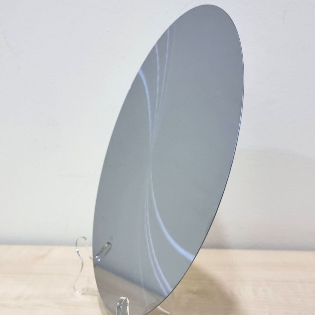
WAFER THINNING SERVICE
Thinning the die can benefit electronic devices in several ways:
The most common technology for wafer thinning is mechanical grinding. Silicon is removed from the backside of the wafer using a two-step process: coarse grinding followed by fine grinding. This is performed using a grinding tool that contains diamond particles of specific dimensions. During coarse grinding, typically 90% of the back grind is completed, significantly reducing the thickness of the wafer. Coarse grinding will cause micro-cracks and damage the silicon lattice. Fine grinding completes the back grind process and removes part of this damage.

