COPPER PILLAR SERVICE

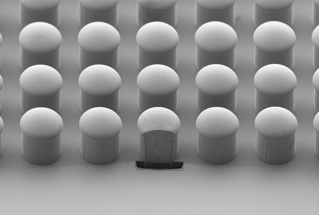
The advance packaging roadmap has demanded for smaller pitch and bump diameter while maintaining the same package height. Cu pillar bumping can cater to the demand of refining package size with better electromigration performance, alongside with other benefits such as RoHS compliance, higher cost efficiency and shorter cycle time.

PacTech offers solution for fine pitch Flip Chip and WLCSP with Cu pillar bumps, our Cu pillar line-up comes with various finishes with individual advantages:

  • Cu Pillar X1 – Basic Cu Pillar for fine pitch Flip Chip
  • Cu Pillar X2 – Cu Pillar with solder cap for better compliance
  • Cu Pillar X3 – Cu Pillar with Ni diffusion barrier
  • Cu Pillar X3en – Cu Pillar with ENIG finish for improved solderability & corrosion resistance

Our Cu pillars come with optional passivation such as PI, suitable for various applications such as 5G & RF, automotive, consumer, power controller and sensor.
Download WLP Brochure
Get in Contact with Sales
Copper Pillar

WAFER LEVEL PACKAGING SERVICES

Electroplating

Electroplating, or electrochemical deposition, is the process of using electrodeposition to coat an object in a layer of metal(s) on any substrate. RDL and Copper for example, are part of this process.

Go to Electroplating Service

Electroless-Plating

Low-cost mask-less chemical deposition of various metal stacks on wafer surface to serve as intermetallic connection or to enhance product reliability and performance.

Go to Electroless-Plating Service

Laser Assisted Bonding

Laser assisted bonding is an interconnection method performed through the laser energy to bond two surfaces of materials together.

Go to Laser Assisted Bonding Service

Solder Balling

Various solder deposition technologies to form solder bump for WLCSP and flip chip interconnects.

Go to Solder Balling Service

Wafer Level Component Assembly

Wafer level assembly by attaching of dies or various passive components on wafer surface.

Go to WL Component Assembly Service

Wafer Thinning

Thinning of wafer backside for dies in final packaging.

Go to Wafer Thinning Service

Wafer Metal Coating

Application of various metal stacks via evaporation or sputtering technologies on wafer backside for better die performance.

Go to Wafer Metal Coating Service

Wafer Dicing

High precision and accurate singulation of dies on a wafer.

Go to Wafer Dicing Service