Electroless Plating Machines for Various Metal Platings
Electroless Plating
In Semiconductor industry, electroless (e-less) plating process is used for finishing bonding pad surface. This pad finishing process provides variety of benefits, e.g. solderability, reliability, and so on. Depending on the pad materials and backend processes, composition of plated metallization needs to be chosen appropriately. Example:
Modular Wet-Bench
The modular wet bench is a compact and flexible wet processing system for the treatment of wafers and panels in plating, etching, stripping and cleaning applications. The system is based on a single process module with two tanks arranged in series and a side-mounted control cabinet. A touch display in the process module as well as a movable central touch monitor provide quick access to status information and process recipes.
After manual loading, a fully automated, integrated robotic arm handles the transport of the carriers from front to rear between the two process tanks as well as the agitation within the tanks. The clear and functional design allows easy access for maintenance and service.
The base unit, consisting of a control cabinet and one process module can be flexibly and indefinitely expanded with additional process modules.
Pac Tech is comprehensive solution provider of electroless plating for semiconductor wafer that has more than 25 years experience in that industry. We will make various proposals based on your needs.


Wafer Level Packaging Service (WLP Service)
As an introductory production, we can offer our subcontracting service/WLP service that is recommended for a mass production without huge investment, a small volume production, R&D and second sourcing.

Plating Line and Plating Chemical
For a mass production at your own facility, we offer you our fully-automated electroless plating line/ PACLINE ® and our plating chemical.

Turn-Key Solution
If you start small volume production with our WLP service and purchase our equipment and chemicals, you can smoothly transition to mass production at your own plant with our proposed turnkey solution. When you install the equipment, we will provide you with a package that includes process recipes and operation training.
Electroless Ni/Au Plating Overview
The Under-Bump-Metallization (UBM) is an integral part of all bumping processes. This layer is typically deposited by physical vapor deposition (PVD), electroplating, or electroless plating. The choice between these three UBM technologies is often dictated by cost and reliability. PVD and electroplating techniques require both high vacuum and photolithography steps and are therefore considered high cost operations. The electroless nickel/gold process technology is a simple wet chemical process that is self-patterning thus leading to lower costs in relation to its total capital investment and operational costs.

Electroless Ni/Au Plating Overview
For copper based semiconductors, the nickel and gold plating baths are the same as those for aluminum based semiconductors. Several acid based cleaning steps are typically used to clean off contaminate and to remove copper oxide from the surface of the I/O pads. The activation step for copper is similar to that used in the laminate board plating industry, and usually uses a palladium based catalyst. The know-how for plating Cu semiconductors is the ability to selectively catalyze the copper I/O pads without activating the surrounding passivation.
This electroless plating processes are inherently low cost, and can be used for a variety of different applications in addition to Flip Chip and WLCSP Bumping, including:
High throughput, and consequently low cost, is accomplished by batch processing cassettes of wafer through an automated electroless plating line. The fact that the nickel plating process is highly selective, and will only plate on the exposed metal surfaces (aluminum or copper), translates into a major cost advantage for this UBM deposition technique. Compared to conventional techniques for depositing the UBM, the use of electroless nickel has the following advantages:
Electroless plating on integrated circuits can, however, be challenging because of the fab-specific variations in materials and processes involved in creating the circuits. Aluminum (or copper) alloy composition, sub-structures under the pad metal, passivation material and quality, pad electrical potential, and energy sensitivity (radiation and grounding effects) all play a role in the plating rates, uniformity, and adhesion of the nickel.
Because the process details (inherent tricks of the trade) are not generally regarded as patentable, developers treat their processes as proprietary. Hence, particulars of electroless nickel plating are not readily available.
The first three steps in the process are critical in determining the overall selectivity of the plating process, nickel morphology, and the adhesion of the nickel to the aluminum (or copper) pad. In general, a process that produces fine grained, uniform, thin layers of the catalyst (zinc or palladium) will produce the best nickel plated structures. The specific chemistries and absolute component ratios are critical in producing this desired structure. In addition to selecting the appropriate plating chemistries, one must also consider availability, place of origin, price, toxicology, bath life, waste treatment/disposal, and environmental issues related to the chemicals when implementing a process in a manufacturing setting.
Electroless Ni/Au Plating Overview
For aluminum based integrated circuits, the chemical sequence for depositing the electroless nickel layer comprises following steps:
Electroless Plating Equipment
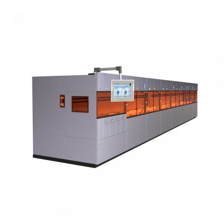
PACLINE ®
The PACLINE ® 300 A50 is a fully automated machine for electroless deposition of Ni/Au, NiPd or NiPdAu bumps on semiconductor wafers.
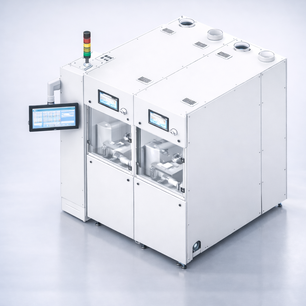
Modular Wet-Bench
The modular wet bench is a compact and flexible wet processing system for the treatment of wafers and panels in plating, etching, stripping and cleaning applications.