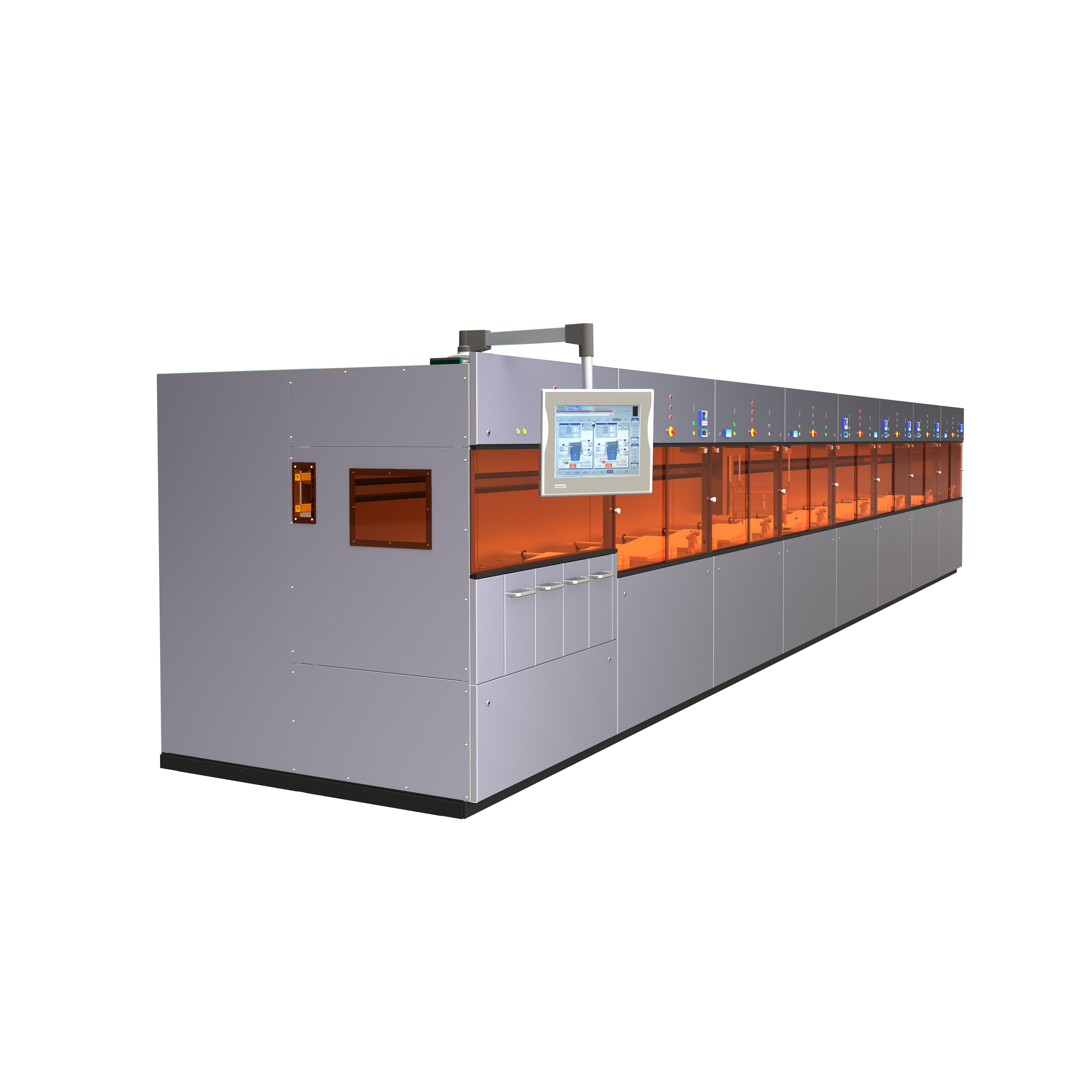
ELECTROLESS PLATING MACHINE WITH HIGH RELIABILITY & QUALITY
PACLINE ®
Our mask-less self-patterning wet chemical plating process applies Nickel, Palladium and Gold over the Aluminium or Copper bond pad on semiconductor wafers of different materials including Silicon, Silicon compound, Indium Phosphide, Lithium Tantalate etc. This layer acts as an adhesion layer, diffusion barrier, and wetting layer for the solders and wire bonds to enhance reliability and performance of various assembly and packaging such as Flip Chip and WLCSP. It uses our specific proprietary chemical compositions for a reproducible and reliable result, which has been proven with over 25 years of our in-house high volume manufacturing experience.
The wafers are loaded in a fully automated wet chemical plating line, where the wafers are handled by robot handler to go through chemical bathes which are well-controlled by in-line analysis and maintenance. Talk to us to understand more about the unique turnkey model we offer for low to high volume production with either subcontracting services or equipment, chemical sales and technology transfer.
Highlights

