ELECTROPLATING SERVICE

Wafer Level Chip Scale Packaging (WLCSP) is becoming more prevalent as industry demands smaller and thinner microelectronic packages. WLCSP allows smaller form factors, improved electrical performance and a relatively simpler structure over conventional wire bond or interposer packaging technologies. PacTech offers state-of-the-art wafer bumping and WLCSP solutions such as RDL and copper pillar plating:
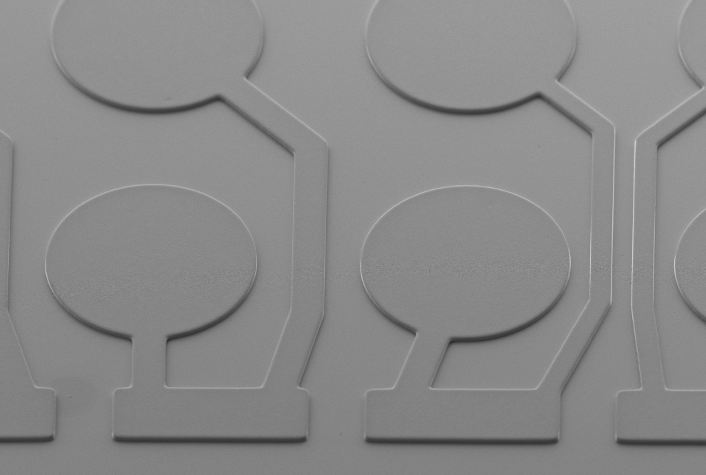
  • Cu pillar bumping with bump diameters as small as 25 microns

  • Possible metal stacks for pillar Cu, Cu/SnAg, Cu/Ni/SnAg

  • Bump-on-pad and bump-on-polymer processes

  • Single and multiple layer Cu redistribution with several polymer repassivation material choices

  • Applicable on Silicon, Glass and GaN substrates, 100mm to 200mm wafer

RDL Redistribution Layer

Electroplating Example (scroll down)

1. Start

The goal is to redistribute the connections placed on an insulation layer. The process starts with a passivation layer on top of the insulation layer.

2. Seed Layer

A seed layer, usualy made of sputtered or evaporated metal, is placed on top of the object to create new connection possibilites.

3. Photoresist

A light-sensitive organic material, the photoresist, is placed on the seed layer. It enables the masking in the next process of photolithography.

4. Photo­lithography

Light is used to mask the photoresist and to generate new patterns for connections. Depending on the polarity of the light, materials with be affected differently regarding weakening and toughening.

5. Electroplating

Into the now masked regions, a thin layer, for example copper or other conductors, is deposited on the seed layer through the electroplating process.

6. Resist Stripping

The mask created through the photolithography is getting stripped from the object so the seed layer can be reworked in the next process.

7. Etching

Undesirable materials, in this case the seed layer, are getting removed from the object, so the seed and copper layer result in the exact same size.

8. Passivation

Deposition of the passivation layer. This separates the new positioned electronical connections after masking in the next process of photolithography.

9. Photo­lithography

The second masking of this process example. On specific positions, the passivation layer gets removed to create new spaces for the under-bump metallization.

10. Electroless UBM

Stacks of metal layers are placed in the masked spaces between the passivated layer to complete the integrated circuit for different applications.

11. Solder Ball

Solder bumps or copper pillars can be now placed onto the UBM layer for subsequent applications like flip chip.

WAFER LEVEL PACKAGING SERVICES

Electroplating

Electroplating, or electrochemical deposition, is the process of using electrodeposition to coat an object in a layer of metal(s) on any substrate. RDL and Copper for example, are part of this process.

Electroless-Plating

Low-cost mask-less chemical deposition of various metal stacks on wafer surface to serve as intermetallic connection or to enhance product reliability and performance.

Laser Assisted Bonding

Laser assisted bonding is an interconnection method performed through the laser energy to bond two surfaces of materials together.

Solder Balling

Various solder deposition technologies to form solder bump for WLCSP and flip chip interconnects.

Wafer Level Component Assembly

Wafer level assembly by attaching of dies or various passive components on wafer surface.

Wafer Thinning

Thinning of wafer backside for dies in final packaging.

Wafer Metal Coating

Application of various metal stacks via evaporation or sputtering technologies on wafer backside for better die performance.

Wafer Dicing

High precision and accurate singulation of dies on a wafer.