To support our team in PacTech Asia in Malaysia, we are looking for a Process Engineer (m/f/d) for the next possible date.

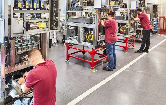
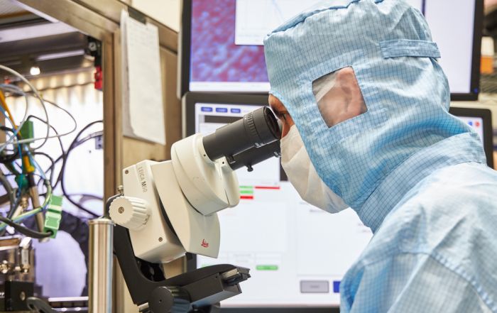
PacTech is a technology-focused company specialized in advanced packaging equipment manufacturing and wafer level packaging services. Since our establishment, our team has been working relentlessly on developing new leading-edge technologies for the next generation applications. We are known to be highly adaptive to customization and unique applications. Our team of technical experts is striving to resolve various packaging challenges faced by the industry to provide our customers and partners more competitive solutions in terms of cost, time-to-market, and technology advancement. Our headquarter is located in Nauen, Germany with two operation and manufacturing sites in Santa Clara, CA, USA and Penang, Malaysia. Together with our sales and field service teams across the globe, we can cater to the demand within your region.

Job Description

  • Work within the team to develop and qualify new products for customers as well as control and maintain processes for existing customer products which are qualified for production

  • Involve in new process and equipment parameters optimization
    – DOE run for process optimisation and parameter windows setting
    – Follow up with the preparation of DOE material and machine parts
    – Collect process performance data and compile engineering reports
    – Equipment conversion and buyoff

  • Perform engineering build (For customer and qual samples)
    – To run process for new product at early stage of engineering build, before handing over to production operator
    – To monitor process performance during engineering build thereafter to release to mass production
    – Provide training and mentorship to operators

Job Requirement

  • Bachelor Degree in an Engineering or Science Discipline with at least 1-3 years of working experience as a process engineer in semiconductor industry

  • Fresh Graduates whom are very determined, willing to learn, a fast learner and have the knowledge about semiconductor wafer (and basic know-how on how to handle the wafers) are welcome to apply as well

  • Hands-on experience in the following process will be given priority consideration:
    1. Wet Chemical Etching, e.g. Silicon Etching or Cleaning
    2. Metal Evaporation or Sputter (PVD)
    3. Wafer thinning
    4. Electroless plating
    5. Electrochemical deposition (ECD) / Electroplating
    6. Photolithography

  • Have some experiences in technologies like thin film deposition, Cu-RDL or Cu-Pillar, or WLP in general

  • Familiar with concepts and documents like FMEA, Control Plan, SPC, Work Instruction etc.
  • Good presentation, communication and team working skills

  • Having “Hands on” attitude and creative problem-solving mind set to get the work done quickly and effectively to meet customers schedules

  • Ability to work under pressure with minimum supervision

  • Applicants should be Malaysian citizens or hold relevant residence status

  • Possess own transport

Address

PacTech Asia Sdn. Bhd.
No. 14, Medan Bayan Lepas, Technoplex, Phase 4, Bayan Lepas Industrial Zone
11900 Bayan Lepas, Penang, Malaysia

Share this Job on Social Media

More Jobs at PacTech Asia