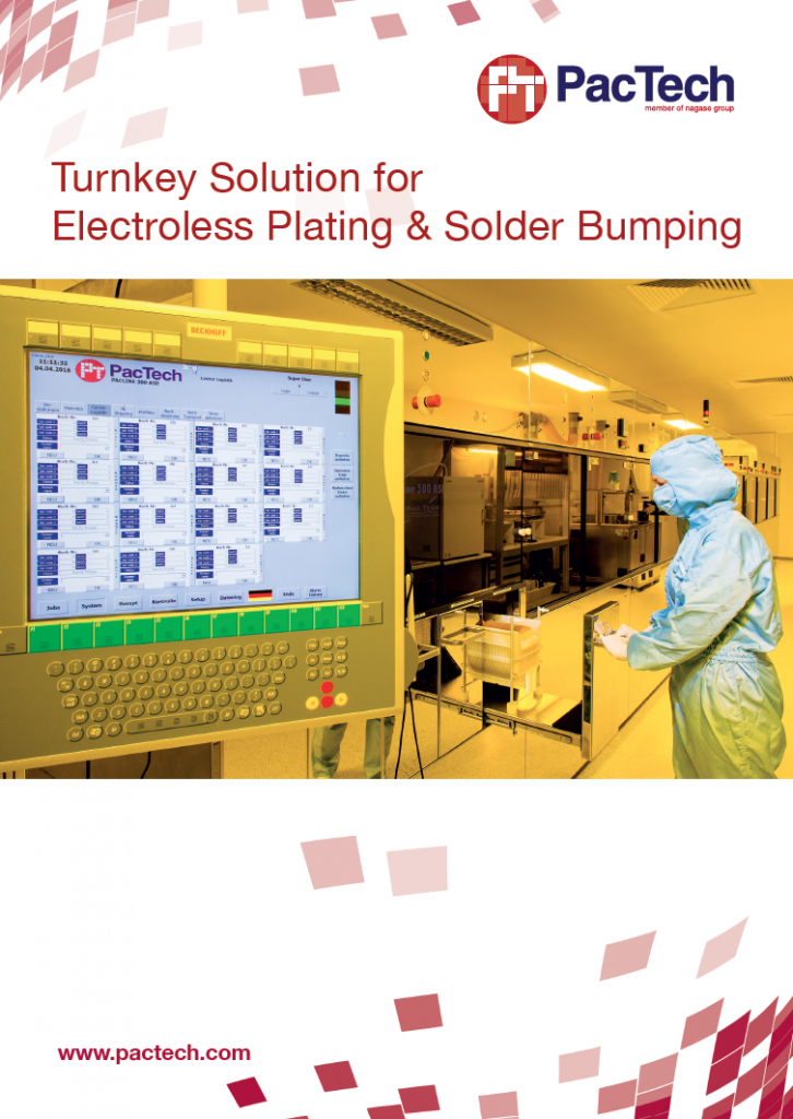
Electroless Plating – Maskless chemical deposition of metal stacks on wafers as intermetallic connection or to enhance product reliability.
Electroplating is the process of using electrodeposition to coat an object in a layer of metal(s) on any substrate.
Electroplated Cu pillar with optional Ni diffusion barrier and SnAg cap for low cost and fine-pitch flip chip interconnects.
Rerouting of pads on a die with metal and dielectric layers to the other locations to fulfil the subsequent packaging rules.
Various solder deposition technologies to form solder bump for wafer level chip scale packaging and flip chip interconnects.
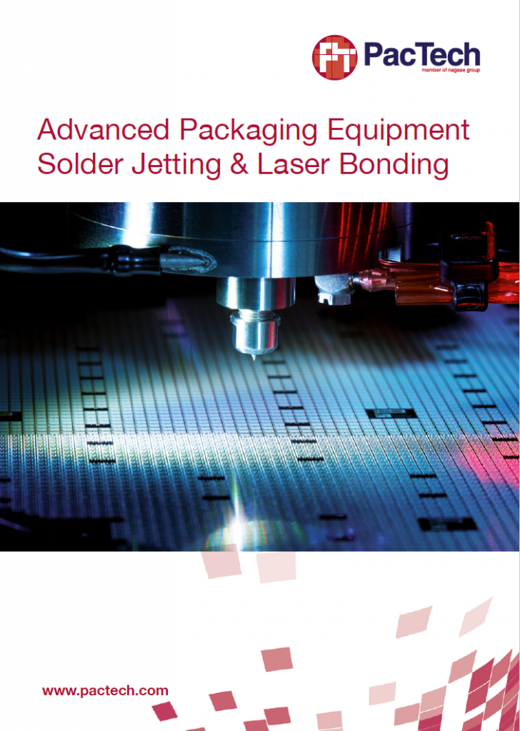
Laser assisted bonding is an interconnection method performed through the laser energy to bond two surfaces of materials together.
We offer wafer level component assembly by attaching dies, chips or various passive components like capacitors on a wafer surface.
Removal of wafer backside materials for thinner die in final packaging via high quality mechanical polishing and chemical stress relief.
Application of various metal stacks via evaporation or sputtering technologies on wafer backside for better die performance.
Wafer dicing is the process where silicon chips (die) are separated from each other on the wafer, accomplished by mechanically sawing.
Click on the download button below to initiate the download.