3D Packaging Machines for Interconnecting Dies/Chips On Wafers
3D Packaging Machines for Interconnecting Dies/Chips On Wafers
3D packaging enables stacking of multiple chips that communicate with each other and is part of 3D integration through horizontal as well as vertical connections. This method provides a more compact way to further improve the performance of a chip while reducing cost and power consumption.
The following methods are used in manufacturing, with various advantages and disadvantages:

3.5D ® Packaging Machines for Interconnecting Dies/Chips On Wafers
3.5D ® Packaging Machines for Interconnecting Dies/Chips On Wafers
PacTech’s 3.5D ® packaging technology pushes the boundaries of conventional 3D packaging by adding an entirely new dimension. This breakthrough approach unlocks unprecedented opportunities to redefine advanced packaging architectures for next-generation high-speed and high-performance applications.
The patented 3.5D ® technology enables seamless vertical integration of additional chips or semiconductor components onto an existing 3D chip stack, allowing functional layers to communicate directly with one another. By dramatically shortening signal paths and minimizing interconnect lengths, the 3.5D ® architecture delivers a significant performance boost. The result is superior signal integrity, lower latency, and enhanced power efficiency, making it ideally suited for AI, HPC, data center, and high-frequency applications.
At the same time, the technology builds on proven interconnection methods: the supporting contacts, routed to the chip edges, continue to rely on conventional solder bumps or copper pillars.
For a detailed technical study on PacTech’s 3.5D ® technology and laser-assisted vertical bonding performance, refer to the publication “Vertical Laser Assisted Bonding for Advanced “3.5 D ®” Chip Packaging” and “Study of Solder Interconnect Configurations & Performance of Vertical Laser Assisted Assembled “3.5 D ®” Packages“.

3D and 3.5D ® Packaging Equipment
3D and 3.5D ® Packaging Equipment
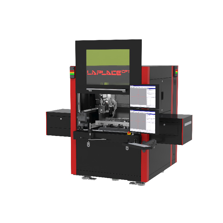
LAPLACE ® – 3.5D ®
The LAPLACE ® - 3.5D ® laser-assisted bonding platform is our solution for ultra-fine-pitch cantilever assembly on wafer probe cards with optional rework capability.

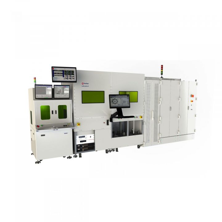
LAPLACE ® – LAR 600A
The LAPLACE ® LAR 600A revolutionizes reflow soldering with laser-assisted technology, offering faster reflow times, reduced thermal stress, and improved efficiency for a wide range of applications, while minimizing energy use and CO₂ emissions.
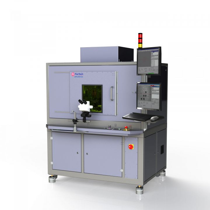
LAPLACE ® – LAB 300A
The LAPLACE ® - LAB 300A provides an integrated solution for flip chip assembly for laser assisted soldering, ACF and NCP interconnections.
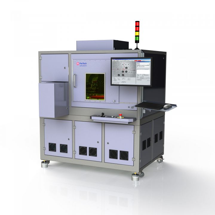
LAPLACE ® – HT
The LAPLACE ® - HT is an automatic Laser Soldering machine for assembly of e.g. Schottky Diodes and Bypass Diodes – especially for solar cell modules.
LAPLACE ® – LAR 600A
The LAPLACE ® LAR 600A revolutionizes reflow soldering with laser-assisted technology, offering faster reflow times, reduced thermal stress, and improved efficiency for a wide range of applications, while minimizing energy use and CO₂ emissions.
LAPLACE ® – LAB 600A
Laser Bonding System (LAB) with compression bonding and laser assisted reflow.