Matthias Fettke, Gero Bonow, Anne Fisch, Moshir Nasser, Georg Friedrich, Rojhat Baba, Thorsten Teutsch
PacTech – Packaging Technologies
Am Schlangenhorst 7-9, 14641 Nauen, Germany
Fettke@pactech.de
Conventional methods of soldering THT-contacts face growing limitations with new-generation products. Finer pitches, more intricate geometries, more excellent aspect ratios, thermally sensitive substrates, and an overall call for a flux-free bonding require different process solutions.
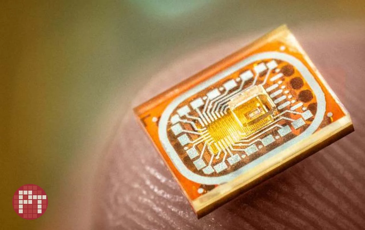
SB² laser assisted solder jetting process addresses these challenges and overcomes them. The process involves jetting a molten solder droplet onto a THT contact. The solder fills the cavity between the pin and the inside of the vertical interconnect access (VIA), forming a reliable mechanical and electrical connection. This pitch-agnostic process works for various 2D and 3D geometries. It has several critical advantages over wave soldering, the conventional industrial solution to soldering THT contacts. Beside the optional use of flux, it supports suitable pitch applications, as the usable solder ball material size can be downscaled to 30 µm. Moreover, it is a gentler process regarding the thermal impact on the substrate. Thermal damage to sensitive substrate parts can be avoided as the substrate heating via contact with the molten solder is highly localized. Furthermore, previous work has proven that interconnect bonds created in such a way are much more resilient against the effects of thermal aging. This is because the thermal event is shorter by 2-4 orders of magnitude compared to the conventional oven-reflow, solder-iron, or wave soldering bonding processes.
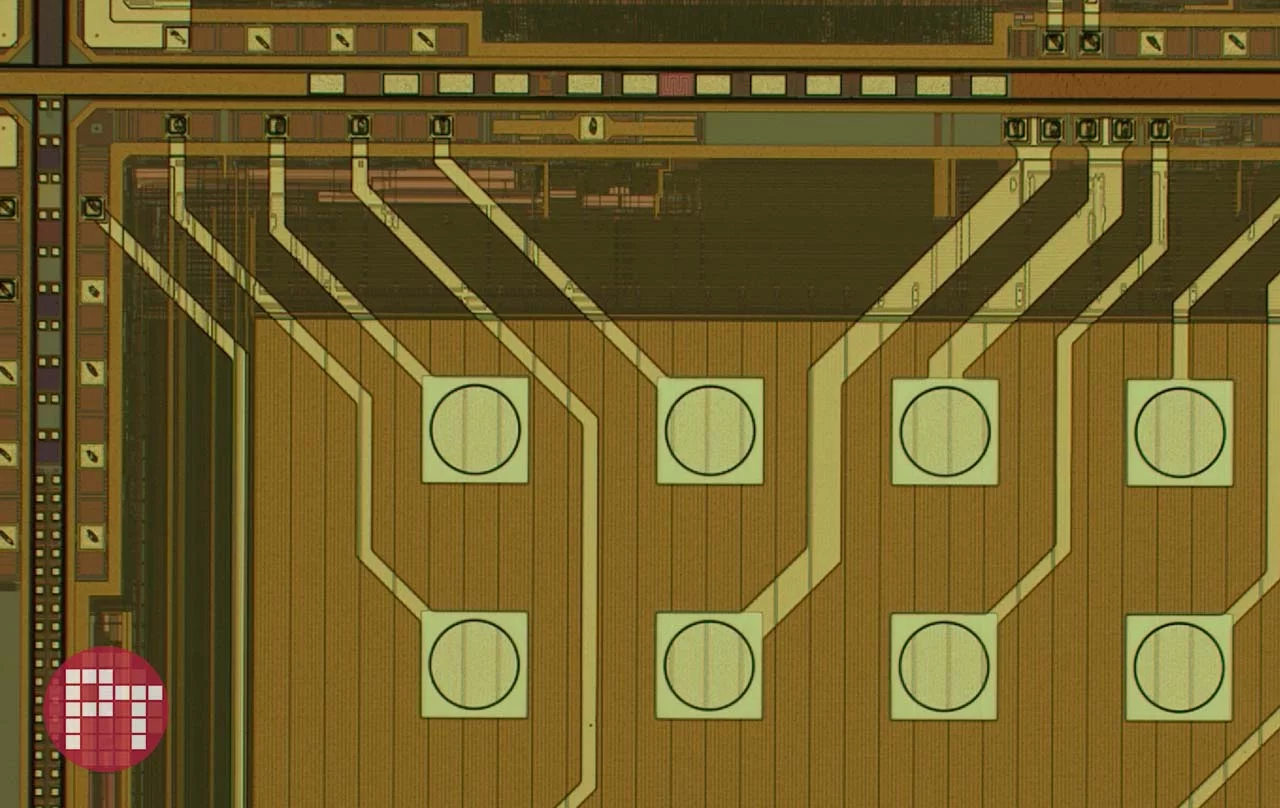
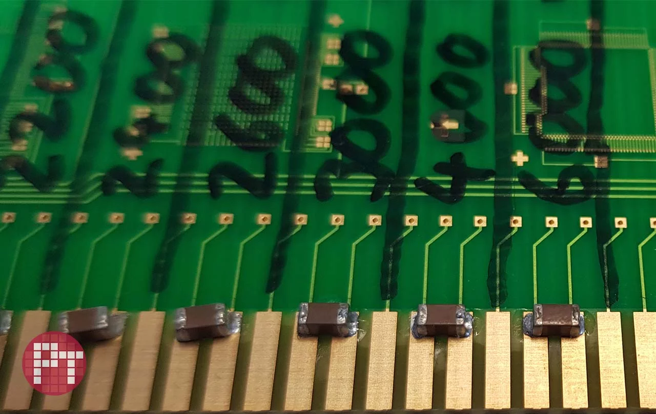
In this work, we created PTH and NPTH THT-contact samples of different geometries and aspect ratios showing various pad metallization (Cu, NiAu, or HASL) and which we then processed with the SB²-Jet method. The resulting test vehicles were subjected to extensive analyses, including microscopic inspection of the bond geometry and X-ray analysis. In addition, the impact on the soldered contacts before and after thermal cycling was microscopically inspected along with metallurgical analysis through cross-sectional polishing.
A model for determining the filling level using a visual scanning system was demonstrated, making the costly and time consuming X-ray analysis or cross-sectional preparation obsolete. Finally, this novel approach’s industrial potential and technological significance are covered, providing an outlook on future technological developments.
Keywords — VIA, TSV, TGV, pin, hole, solder, interconnect, THT, SMT, packaging, flux-free, laser