By: Kevin Kröhnert, Georg Friedrich, Dzmitry Starukhin, Markus Wöhrmann, Michael Schiffer, Martin Schneider-Ramelow.
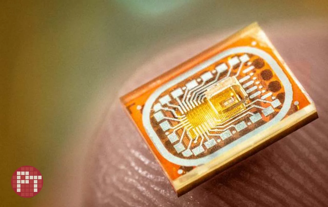
In this work we present aspects of our versatile hermetically sealed sensor platform. The sealed glass package can include passive and active devices (radar, pressure, infrared sensors). Glass is used due to its ideal properties for such applications, like excellent chemical resistance, mechanical strength and low costs. The hermetic sealing allows seamless operation in hazardous environments. The tgvs (Through – Glass – Vias) may be deployed, for instance, in iniaturized sensor systems as vertical DC and RF interconnections with reduced parasitics for improved performance of the sealed device, while maintaining hermetic sealing. Tgvs improve the performance drastically and will provide a hermitically sealed connection to the inner circuitries of the package. This approach was previously compared regarding their RF properties to the conventional approach and showed superior properties with less effort for fabrication [1] [2] [3].
In this paper we focus on three aspects of the package, the wafer-to-wafer bonding techniques for the sealing of the package, the reliability of the tgv integration in the interposer, and the heat dissipation through the tgvs. For the sealing, SAC 305 solder balls are used. Using the Pactech SB²-Jet high-speed sequential solder-ball attach and laser reflow process, we are able to create a continuous layer of solder around a seal ring and place a solder ball on top of each I/O (Input/Output) pad. The pads are used to transmit signals from the bottom of the interposer to the top wafer, which will then contact the ASIC pads. The system is capable to singulate, to position and to reflow solder balls with a diameter between 40 µm and 760 µm. A big variety of different solder material e.g. SnAgAu, SnAu, InSn, SnBi is applicable. Due to the use of a laser reflow process no flux is needed.
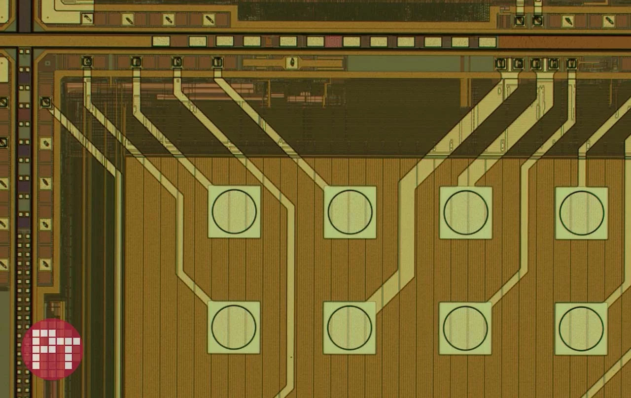
For wafer bonding, a wafer-to-wafer bonder is utilized to heat the wafers and bring them into contact. To create a defined separation between both bonding partners, spacers had to be applied. A specific amount of copper filled solder balls are placed with the SB² Jet to achieve a defined distance between both wafers. The alignment accuracy of both wafers was sufficient and a fair amount of solder was squeezed out. To evaluate the tgvs in their electrical and thermal behavior a separate layout was designed. We used daisy chains, kelvin structures, micro strip lines and capacitive structures to evaluate all relevant parameters. The wafers where then electrical tested and where put through thermal cycling to see how well the tgvs will perform. An overview of all the achieved good results will be presented in the following paper.