Wafer Bumping Machines for Assembly Process Interconnections
Wafer bumping is often separated into two different categories: Flip chip bumping (FC) and wafer level chip scale packaging (WLCSP). This categorization and affiliated nomenclature is partially based on the solder bump size and the type of equipment used to create the bump.
The basic flow for each of these technologies is to first deposit a barrier metal on top of the bond pad of the wafer (Under-Bump Metallization or UBM) followed by deposition of the solder. Possible Solder Alloys:

Wafer Bumping Equipment
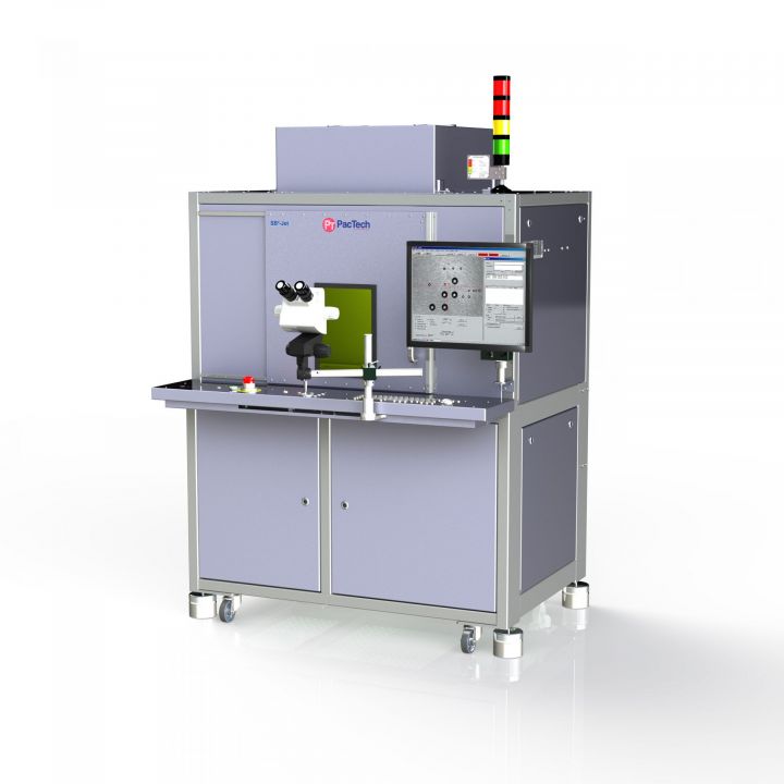
SB² ® – Jet
SB² ® - Jet은 PacTech의 SB² ® 시리즈 중 가장 높은 배치 정밀도를 제공하며, 가장 작은 솔더 볼까지 처리할 수 있습니다.
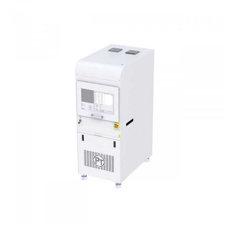
SB² ® – Compact
SB² ® - Compact 장비는 고도로 유연하고 초소형 워크스테이션을 갖춘 대량 생산용 SB² ® 시리즈의 입문형 설비입니다.
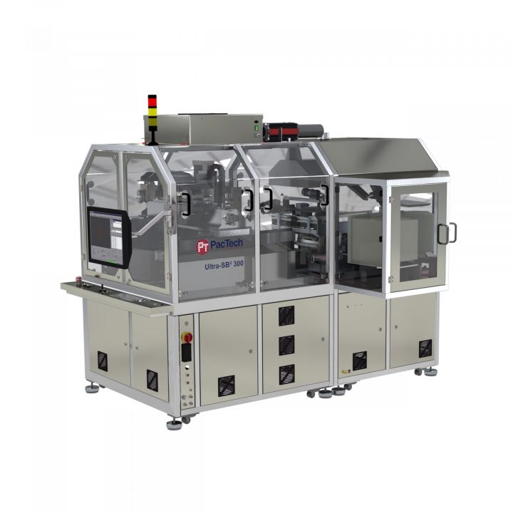
Ultra-SB² ®
Ultra-SB² ® 는 플럭스 프린팅, 볼 마운팅, 2D 검사 및 웨이퍼 레벨 리웍를 통합한 완전 자동화 솔더 범핑 설비입니다.
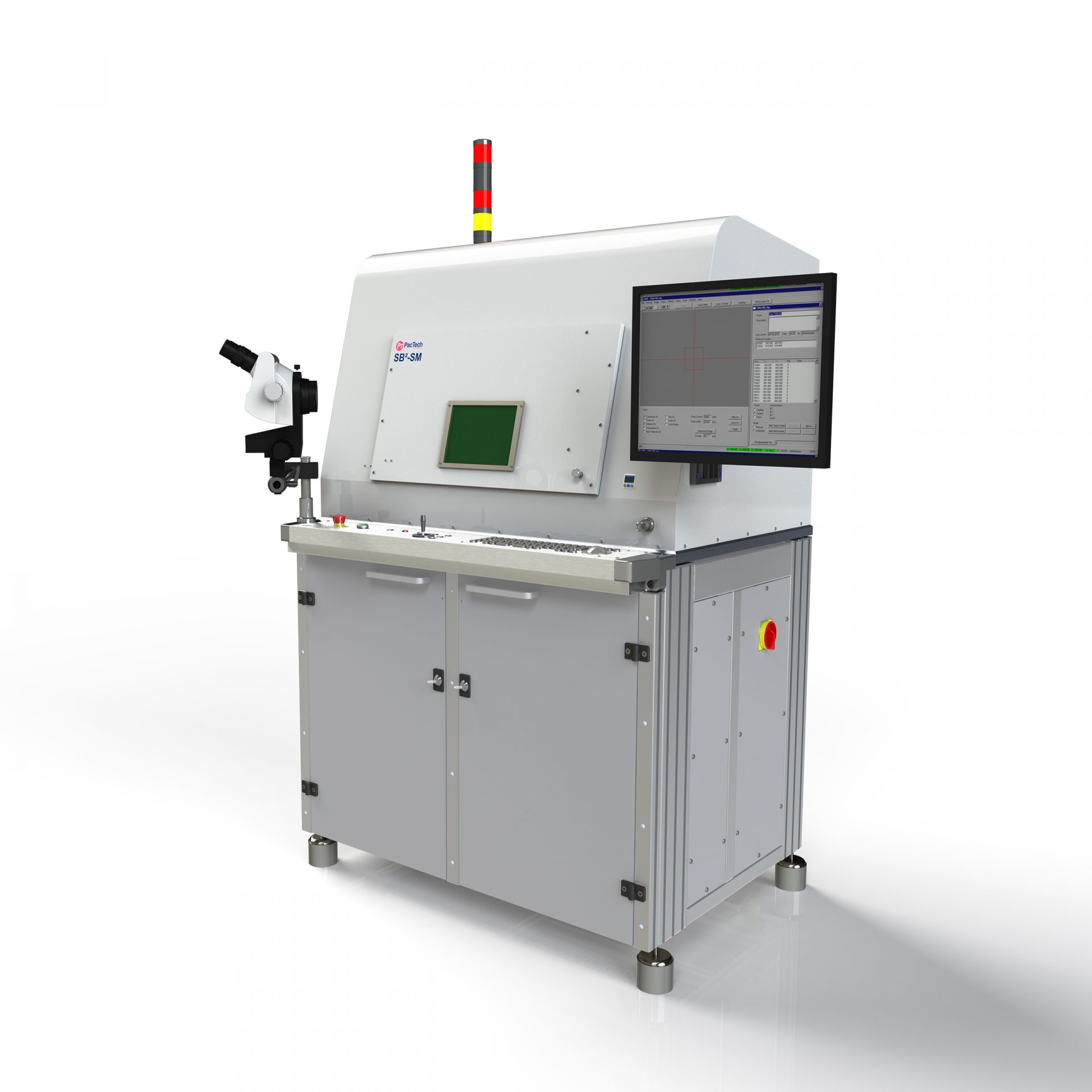
SB² ® – SM
SB² ® - SM은 프로토타입 제작 및 소량 생산을 위한 장비로, SB² ® - M보다 넓은 작업 영역과 더 다양한 선택 기능을 제공합니다.