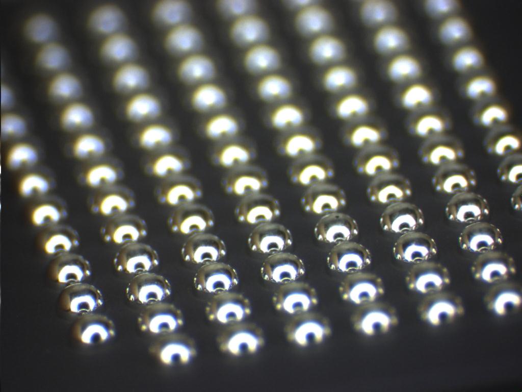
Wafer Bumping Machines for Assembly Process Interconnections
Wafer bumping is often separated into two different categories: Flip chip bumping (FC) and wafer level chip scale packaging (WLCSP). This categorization and affiliated nomenclature is partially based on the solder bump size and the type of equipment used to create the bump.
- “Flip Chip” refers to bumps on semiconductor wafers which are in the range of 50 to 200 µm in height and are usually assembled using and underfill material between the die and the substrate.
- “WLCSP” refers to bumps that are in the range of 200 to 500 µm in height and are usually assembled without an underfill material.
The basic flow for each of these technologies is to first deposit a barrier metal on top of the bond pad of the wafer (Under-Bump Metallization or UBM) followed by deposition of the solder. Possible Solder Alloys:
- SnAgCu (SAC305, SAC405, SAC105)
- SnAg
- PbSn 95/5, PbSn 90/10
- AuSn 80/20
- InSn
- SnBi


