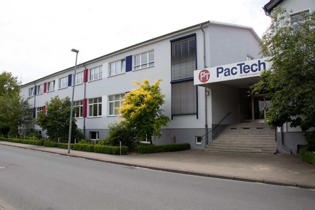
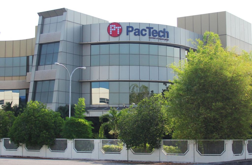
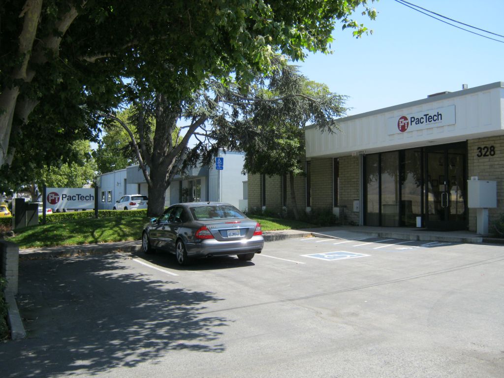
Locations and Certificates of PacTech Facilities

PacTech – Packaging Technologies GmbH
Address
Am Schlangenhorst 7-9
14641 Nauen
Germany
+49-3321-4495-100
Services
- EQ Production
- Bumping Service
- Customer Support
- Sales
Certificates
- ISO9001
- IATF16949
- ISO14001
- ISO50001
PacTech Asia Sdn. Bhd. 200601035342 (755101-P)
Address
Plot 14, Medan Bayan Lepas Technoplex
Phase 4 Bayan Lepas Industrial Zone
11900 Bayan Lepas, Penang
Malaysia
+60-4-644-0986
Services
- Bumping Service
- Customer Support
- Sales
Certificates
- ISO14001
- ISO9001
- IATF16949


